 +565 975 658
 info@premiumcoding.com
 Monday - Friday, 8.00 - 20.00
Graphene is regarded as one of the new generation electronic materials because of its excellent chemical stability and remarkable electron mobility at room temperature. However, the growth of graphene usually need high temperature and metal catalysts, which has greatly limit the application of graphene in the semiconductor devices. So far, as best as our knowledge, there is no technology which allows high quality nitrogen doped graphene (NG) crystals to be grown directly on dielectrics at low temperature.
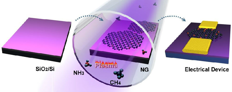
By improving the plasma-enhanced chemical vapor deposition method, Wei’s group and their cooperators from the National University of Singapore, have developed a new technology to grow large-area NG at critical equilibrium state between the competitive processes of nucleation and etching. This new method enable to grow NG directly on dielectrics at temperatures as low as 435 ℃, which solved the problem that NG grown by existing methods cannot be used directly to electrical devices. NG prepared by this method shows an n-type behavior and a high carrier mobility. More importantly, this method has good compatibility with the existing semiconductor technologies, and we believe that this method will promote the application of graphene in the semiconductor industry.
The work was published on ACS Nano, see details: Dacheng Wei* , Lan Peng, Menglin Li, Hongying Mao, Tianchao Niu, Cheng Han, Wei Chen, and Andrew Thye Shen Wee, Low Temperature Critical Growth of High Quality Nitrogen Doped Graphene on Dielectrics by Plasma-Enhanced Chemical Vapor Deposition, ACS Nano, 2015, 9 (1), pp 164–171.
Article links:http://pubs.acs.org/doi/abs/10.1021/nn505214f

Get to know us better now!

Wechat:FDUMMers
Search!
Search across our website
Revenant @ 2018 by fudan | All Rights Reserved
Powered by Weicheng

